



AI semiconductor manufacturing is changing what engineers in a chip factory can do, and how fast they can do it. Demand for advanced chips is rising, the processes used to build them are getting more complex, and the margin for error is shrinking. Some of the analyses engineers need — understanding how a process change will behave, how a material will interact with a new step, or how a defect maps back to a root cause — can take days. Physical experiments on a fab line are slow and expensive, and a wrong call on yield or process quality has real consequences. That combination is why AI has found a practical foothold in the fab: not as a replacement for engineers, but as a way to shorten the wait between a question and a usable answer.
The idea NVIDIA uses for this shift is the AI-defined fab: a semiconductor manufacturing factory where AI helps engineers optimise processes, catch problems earlier and make better decisions across the full chip manufacturing lifecycle. It rests on four capabilities working together: faster simulation, physics-based prediction, AI agents that carry out sequences of engineering tasks, and digital twins that let teams test changes virtually. Each one answers a different bottleneck. Together, they describe a factory where production data informs models, models evaluate changes, and engineers — still the decision-makers — act on what they learn sooner.
AI semiconductor manufacturing and the AI-defined fab
It helps to start with what an AI-defined fab is not. It is not a factory run by AI, and it is not a claim that engineers have been removed from the process. In the picture NVIDIA and its partners describe, engineers direct the work and make decisions based on their expertise, while spending less time waiting for answers. The AI does the slow, repetitive or computationally heavy parts: running a simulation, estimating how a process will behave, selecting a model for a task, or testing a layout change in a virtual factory.
That distinction matters because each capability has a different job, and a different limit. Faster simulation does not make a bad process good; it lets engineers compare more alternatives before committing to a physical trial. Prediction does not replace a full simulation in every case; it offers a fast estimate where a full calculation would be too slow to be useful. Agents do not decide what should happen; they carry out the steps between decisions. Digital twins do not remove the risk of a factory change; they let teams discover problems in a virtual environment first. Keeping those jobs separate is the clearest way to judge the claims that follow.
Faster simulations let engineers test more alternatives

Accelerated computing does not just speed up individual calculations. It changes how many alternatives engineers can test before committing to a physical trial, and in some cases it expands what engineers can verify before production. That is the first, most straightforward part of the AI-defined fab: the same simulation, run faster, becomes a different kind of tool.
Multiphysics simulations are a good example. They model interactions among physical effects such as heat transfer, electrical behaviour and mechanical stress, which is exactly the kind of coupled problem that appears when optimising semiconductor equipment and processes. Using the NVIDIA cuDSS library, multiphysics software provider COMSOL is accelerating such simulations for semiconductor manufacturing by up to 10x, according to NVIDIA. That helps engineers optimise equipment and processes, compare alternatives and decide which changes are worth testing physically.
Applied Materials reports similar gains in materials and process work. By integrating NVIDIA cuDSS, its Ginestra simulation platform runs up to 10x faster than CPU-only approaches. And with NVIDIA PhysicsNeMo, Applied’s ACE+ multiphysics platform delivers topography simulations up to 35x faster. Topography — the shape of surfaces and structures being built up on a wafer — is a case where a faster simulation directly expands what engineers can explore about a process before they commit to it.
Computational lithography shows the other side of acceleration: enabling a calculation, not just shortening it. Lithography defines how circuit patterns are printed onto silicon, and accelerating selected lithography workloads reduces runtime constraints and enables more comprehensive optimisation before tapeout. Siemens is integrating NVIDIA cuLitho into its Calibre lithography software, and NVIDIA reports up to 17x acceleration on key simulation workloads. Siemens’ own announcement gives a related but different figure — up to 12x for full-chip optical proximity correction workloads — with verified engineering data ranging from at least 10x to 17x across selected workloads. The figures are not contradictory; they measure different workloads. What they share is the practical point: engineers can verify more before a wafer goes to print, and identify potential hotspots before tapeout.
Physics-based AI predicts behaviour without a full simulation
Acceleration is one thing; prediction is another. AI trained on physics can predict how materials and processes will behave without running a full simulation each time. The payoff is most visible in complex calculations that are expensive even on accelerated hardware, where running the full model for every candidate condition would still be too slow.
Plasma is the clearest example in the sources reviewed. Plasma is the electrically charged gas used in semiconductor etch processes, and modelling its behaviour requires solving equations that capture how electrical, chemical and thermal processes interact. That makes repeated simulation costly. Lam Research demonstrated that the NVIDIA PhysicsNeMo framework can predict plasma behaviour in milliseconds, compared with days for a full simulation, giving engineers a faster way to explore process conditions without rerunning the full model each time.
The same idea extends beyond plasma. Physics-based models can estimate material and process behaviour without running a full simulation each time, and Applied’s topography work shows prediction and acceleration working together rather than as rivals. But the limit is important, and it is built into the claim itself: a prediction is an estimate trained on physics, not a replacement for a full simulation in every case. The supplied evidence does not determine when a full simulation or a physical trial is necessary or sufficient, so where accuracy matters most, or where a process moves outside the conditions the model was trained on, remains a question for validation rather than an established rule. The sources reviewed do not settle exactly where that line falls, and that is a question research and production experience still have to answer.
AI agents handle the steps between decisions
Engineers turn analyses into decisions: revising a design, investigating a test failure, adjusting a production process. AI agents, in this setting, help carry out the steps between those decisions. That framing matters. The agent is not deciding whether a process change is right; it is doing the sequential work that sits between one human decision and the next.
Advantest provides the concrete example. Evaluating which AI model to apply to a given task is a sequential, manual process that can consume hours on the test floor. Advantest is using NVIDIA NeMo Switchyard AI agents to automate that selection, reducing response times from hours to minutes. The human decision — what to do with the result — remains. What changes is how long the preparatory sequence takes.
This is also where earlier Agentic Affairs coverage of agents connects most directly to the fab. An agent that selects a model, calls a tool and reports back is running the same basic loop as an agent in any other workflow: take a goal, break it into steps, use tools, check results and adapt. In a fab, the stakes of a wrong step are physical — a wasted trial, a yield problem, a process change that should not have shipped — so the checkpoint matters as much as the speed. The agent earns its place by making the sequence faster and more repeatable, not by removing the engineer who judges its output.
Digital twins let teams test factory changes before the line
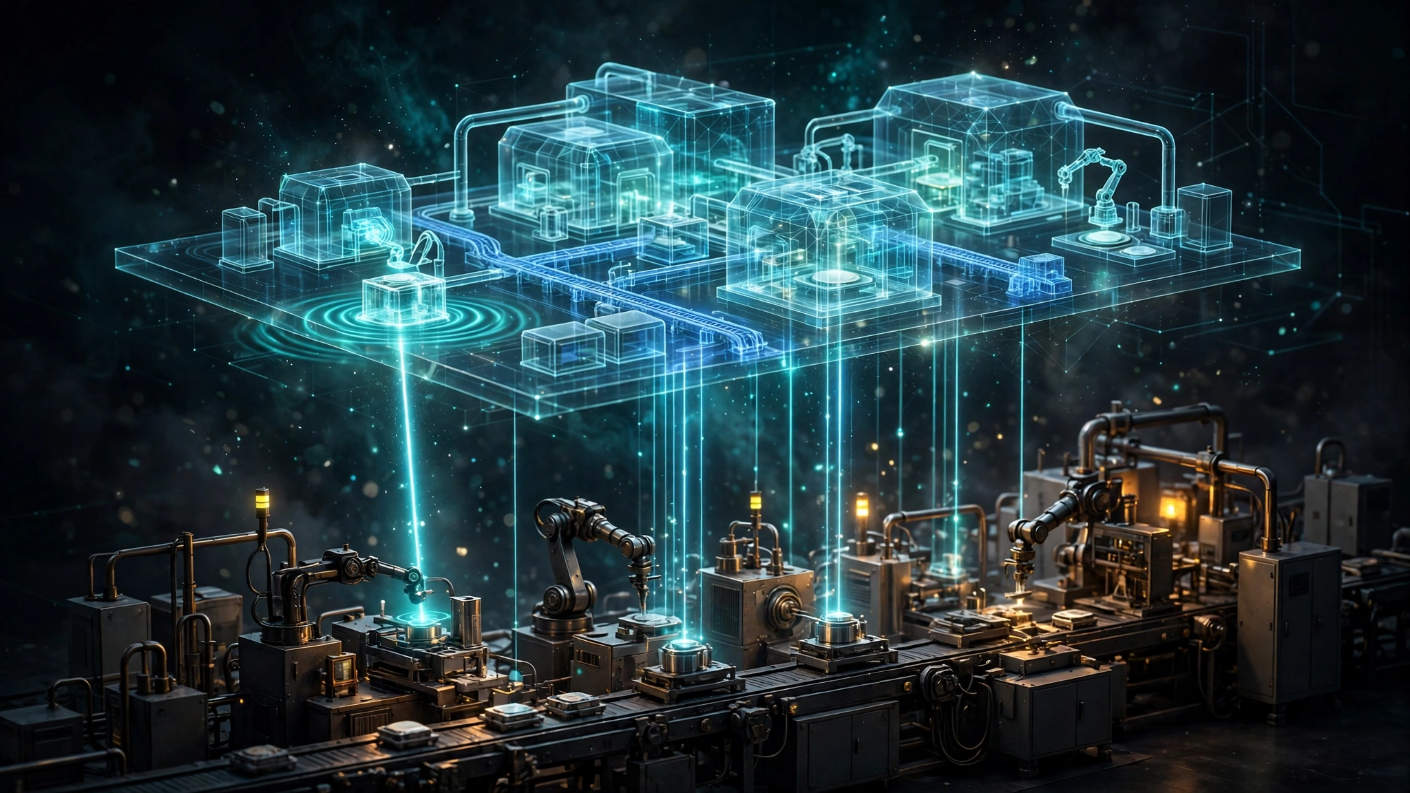
Digital twins extend the same idea from a single process to the whole factory. A digital twin is a virtual model of a physical system that teams can test changes in before committing to physical trials. In a fab, that means simulating equipment configurations, layouts and process changes in a virtual environment, which reduces experimentation costs — especially as fabs become more complex and the stakes of a wrong change get higher.
Applied Materials uses NVIDIA Omniverse libraries to build physically accurate digital twins of entire fabs. Teams can simulate material movement, identify bottlenecks and evaluate layouts and operating strategies, extending virtual experimentation beyond individual processes to how the factory works as a whole. NVIDIA also describes a photorealistic fab digital twin, built with Omniverse libraries and pictured with Applied Materials as the source, used to simulate material flow, spot bottlenecks and validate operational strategies before deployment.
The value here is not just avoiding a bad physical trial. It is being able to ask questions about the factory as a system: what happens to material flow if a layout changes, where does a bottleneck move, which operating strategy holds up under different conditions. Those are questions that are hard to answer by testing one process at a time, and expensive to answer by rearranging a real fab. A twin lets a team explore them first, then commit physical time and money to the changes that survived the virtual test.
The connected loop — and its limits
The future NVIDIA describes lies in connecting these capabilities: using production data to inform models and models to evaluate changes, then bringing those findings back to the engineers making production decisions. That is the connected loop, and it is the promise of the AI-defined fab in one sentence: AI helps people learn from each production cycle and act on that knowledge sooner.
It is also where honest reading matters most. Nearly all of the specific figures in this article come from NVIDIA and its partners: COMSOL, Applied Materials, Siemens, Lam Research and Advantest, as reported by NVIDIA, with Siemens’ own announcement corroborating the lithography work. Independent reporting on the Siemens announcement notes an important scope limit: speedups of 10x to 17x concern particular computational tasks, and they do not establish an equivalent acceleration across the complete chip manufacturing process or guarantee identical improvements for every customer configuration. That caution applies, in spirit, to the other figures too. A 35x topography simulation or a plasma prediction in milliseconds is a result on a specific workload, not a claim that the whole fab runs that much faster.
Several questions also remain open in the sources reviewed. The accuracy limits of physics-based prediction — when a fast estimate is good enough and when a full simulation is still required — are not settled by a single demonstration. Some capabilities described in the wider announcements, such as Lam Research’s NanoVDB-accelerated wafer-etch modelling, are targeted for release by the end of this year rather than already shipping, so their production status differs from the simulation gains already reported. And the sources reviewed do not disclose what adoption costs, or what it requires, for fabs that are not large vendor partners. Those gaps do not cancel the underlying shift, but they do set its pace: AI semiconductor manufacturing is changing the fab first where simulation, prediction, agents and twins remove a specific bottleneck, and the connected loop is a direction of travel, not yet a finished factory.